Copyright © 2020-2021 Shenzhen CDTech Electronics LTD. All rights reserved. Site Map Powered by iwonder.cn

display / touch / bonding solutions
display / touch / bonding solutions
A display module rarely fails EMC testing because the panel is noisy. It fails because the assembly turns a flex cable and a clock line into an antenna, or because pre-compliance stopped at the wrong measurement. This guide follows the sequence that isolates the cause: clock margin first, then harness, grounding and shielding, and only then a decision about the panel or the interface. It assumes the assembly is being prepared for EN 55032 emissions and EN 55035 immunity, with an accredited test slot already booked.
An LCD panel is large, slow and low-current, so it is seldom the strongest radiator on the bench. The flex feeding it is a different object: a long flat conductor carrying a fast clock, its return a fraction of a millimetre away, the pair running parallel to the panel's frame. That geometry has real loop area and a length near a quarter wavelength in the VHF band, where the first radiated failures appear.
When a scan shows a harmonic family rather than a single spike, the FPC usually closes the loop, not the glass. It is why swapping one panel for another with the same flex and pinout changes very little: the antenna did not change. The flex deserves direct measurement, because its shape, length and termination remain under the design team's control. The regulatory path is summarised on the site's page on EMC certification for display products.
Class A and Class B describe the environment the finished equipment is installed in, not the panel inside it. Class A covers commercial and industrial locations. Class B covers residential locations, and its radiated limits sit roughly 10 dB below Class A in the same tables. A display assembly sold to an industrial integrator is normally tested in the class of the end product, often Class A. The same assembly in a domestic appliance, a shop terminal or a clinic console follows the stricter class.
The decision belongs in the test plan before the first scan: a result that passes Class A by 4 dB is a Class B failure. Define the class from the installation environment and the end-product documentation, then label every pre-compliance limit with the class it came from. The legal texts are the EU EMC Directive 2014/30/EU, the UKCA marking guidance and, for North America, 47 CFR Part 15.
The first measurement is not a scan of the whole assembly. It is the pixel clock and its first harmonics, probed at the connector pin field, the middle of the flex and the edge of the shield can. A clock in the tens of megahertz places its lower harmonics inside the 30 MHz to 1 GHz radiated band, so the same family appears at all three positions. What changes is which part of the structure radiates it.
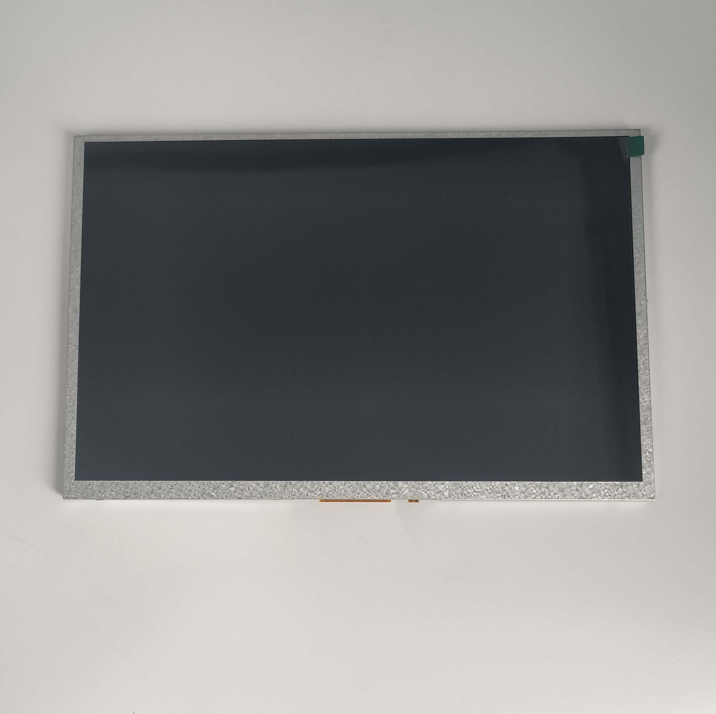
Drive the panel with the pattern the accredited lab is likely to use, not a white screen, then compare with the display powered and the LVDS pair idle. If the family persists with no data, the clock is coupling before the receiver. If it collapses, the coupling depends on data activity and the pattern becomes part of the test setup. Pinouts and LVDS variants are collected in the guide to display interfaces and controllers.
Order matters more than the individual steps, because each one removes a class of cause and the next only makes sense once the previous one is clean. Change one variable at a time and record the configuration with every sweep. A sequence followed consistently produces comparable scans; one that jumps between fixes produces plausible stories and no evidence.
Six decibels is a common internal target for a first pass, and ten decibels is safer for a design that still has mechanical changes pending. The gap covers measurement uncertainty, the difference between an in-house set-up and the accredited lab, cable layout, table height and the worst-case pattern the lab may choose.
Margin also has to survive production. If the only way to reach 6 dB is a ferrite that cannot ship on the final harness, the margin is not real. Prefer changes that survive cost review: a shorter flex, a better connector pinout, a bonded bracket. Record the class, the distance and the configuration next to every number, since a margin without its conditions cannot be compared with the lab result. The verification context is set out on the site's quality and certifications page, and the test house's scope is worth checking through a body such as BSI Group.
Most harness changes move a radiated result by shifting loop area or the common-mode return, and they differ widely in cost. The table lists the changes worth trying, the effect they usually have and when they remain available.
| Harness change | Typical effect on a radiated result | When it is worth doing |
|---|---|---|
| Shorten the flex by 20 to 30 mm | Moves resonances up, often lowers 100 to 300 MHz | Late in the design, while the flex outline is free |
| Add ground pins between clock pairs | Reduces loop area and crosstalk | At the connector definition stage |
| Clip a ferrite at the connector | Attenuates common-mode current above 30 MHz | For diagnosis, not production |
| Route the flex away from a chassis seam | Removes a resonant slot from the coupling path | Whenever the layout allows |
| Bond the bracket near the connector | Gives common-mode current a short return | When the bracket is already metal |
Read the table as hypotheses, not a menu: a change that lowers the whole band acts on the common-mode path, while one that shifts specific peaks acts on a resonance. The IEC Webstore confirms the current edition of the test method.
A shield is only as good as its termination. Foil wrapped around a flex and drained through a single wire is an inductor in series with the shield, and at 300 MHz that inductance is the difference between a shield and a decoration. The termination has to surround the conductor: a metal shell clamped around the flex, a connector with a full perimeter ground, and stitching between the shell and the chassis panel.
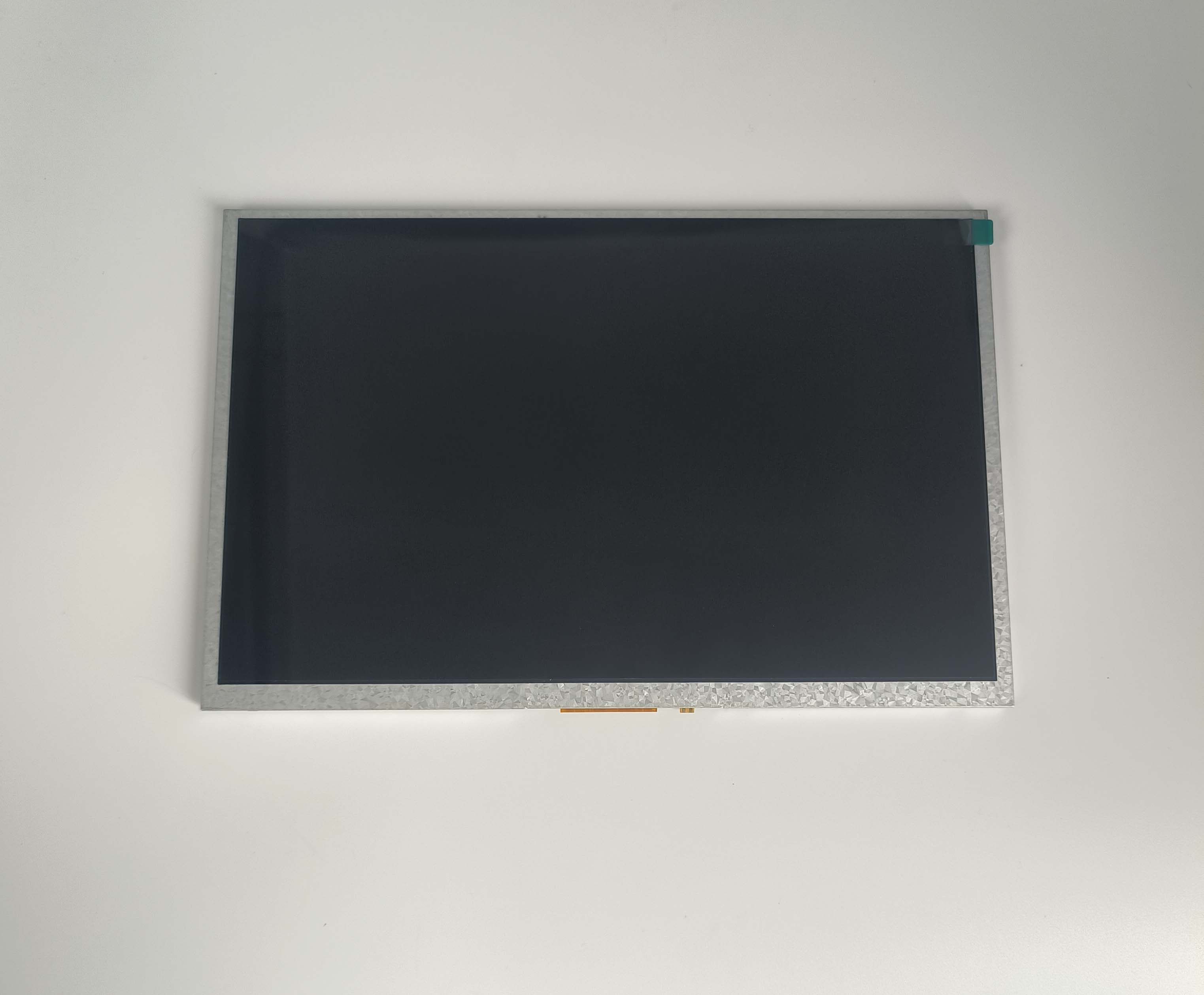
Stitching is where most assemblies lose the benefit. The shield is bonded at one corner, the chassis has a painted seam 15 mm away, and the return current takes the long path around the opening. Vias or spring fingers spaced closely along the connector edge keep that path short. Check the bond with a milliohm meter rather than by eye, because paint and plating thickness are invisible in a photograph but decisive at radio frequency.
Yes, usually: immunity shifts more than emissions.
A touch sensor adds a second flex, a scan controller and a floating plane, so ESD and RF fields find new coupling paths more readily than harmonic content changes.
The sensor stack adds a conductive plane in front of the panel, a controller running its own scan bursts and a second flex that often runs parallel to the display flex. ESD now reaches the touch controller before it reaches the display connector, and a radiated field can be rectified at the sensor edge rather than at the panel. In EN 55035 terms the pass criterion shifts: a display with a clean picture can still fail because the touch function resets, reports ghost coordinates or loses a finger during the disturbance.
Emissions are less affected because scan bursts are low duty cycle and narrowband, so they appear as low-level content, not a new harmonic family. The exception is a controller whose scan clock sits close to a display clock harmonic, where the two add in phase. Test immunity with the layer fitted, and treat touch function as part of the performance criterion.
A shielded flex lowers the total emission, and that is the problem: the number improves enough to look like progress while the dominant path stays open. The residual radiation comes from the shield's own termination, the connector shell to chassis bond, or another structure such as the backlight driver or a board-to-board connector. The shield has not fixed the coupling; it has reduced one contributor and removed the signature that identified the others.
Measure the shield as a variable rather than a cure. Run the same scan with the shield fitted, removed, and fitted again but terminated at one point only. If the shielded and unshielded results differ by less than a few decibels, the flex was never dominant. If single-point termination is nearly as good as the full perimeter, the shield is not carrying the current that matters. Either outcome redirects the work to the chassis before a mechanical change is committed. The rework consequences are covered in the site's quality and reliability guide.
Three failure patterns account for most repeat work on display assemblies, and each points at a different coupling path. Reading the pattern before choosing a fix separates a two-day iteration from a two-month one. The table pairs each pattern with its usual path and the smallest change that confirms the diagnosis.
| Failure pattern | Most likely coupling path | First fix to try |
|---|---|---|
| Broadband rise from 30 MHz, no distinct peaks | Common-mode current on the display harness | Clamp the harness, bond the connector shell |
| Harmonic family locked to the pixel clock | Loop area between signal and return | Rework the flex return, add ground pins |
| Peaks that move when the frame is pressed | Shield can contact and chassis seam | Restore perimeter bonding, stitch the seam |
The three failures that recur are not three panel defects. They are a loop the flex closes, a class chosen too late and a shield that was never terminated. Each is visible in a pre-compliance scan long before the accredited date, if the scan runs in a fixed order and the configuration is recorded.
The configuration, the clock margin and the harness.
A test plan that lists standards but not configuration invites a repeat visit. State the panel, the driver, the backlight and the exact harness length that will be tested, because radiated emissions follow the cable rather than the datasheet. Record the resolution and refresh rate that will run during the scan.
Three further items earn their place: the pre-scan clock margin you measured, so the laboratory knows what headroom it is inheriting; the enclosure material and any apertures, since a metal jig and a plastic bezel behave differently; and the touch overlay, which changes both the ground path and the immunity result. A plan carrying these can be quoted and scheduled. One without them cannot.
If the sequence above has narrowed the problem to the flex, the connector or the shield termination, the next step is a layout conversation rather than another scan. CDTech can review the interface definition, the FPC outline and the grounding scheme against the panel it supplies, so changes are settled before the accredited test date. Write to [email protected] or use the contact page.
Which limits apply to an industrial panel, Class A or B?
The panel itself has no class. EN 55032 applies to the finished multimedia equipment, so the class follows the installation environment declared for that equipment. Industrial and commercial installations normally use Class A, while equipment intended for residential use, including many point-of-sale and clinic products, uses Class B, whose radiated limits sit roughly 10 dB lower. An integrator who buys an industrial panel but sells a product into homes must meet Class B, and the display assembly has to be designed for that from the start.
Can a shielded FPC fix radiated emissions?
Sometimes, and often only partly. A shield on the flex reduces the loop that radiates, so harmonics tied to the pixel clock usually drop. If the dominant path is common-mode current on the harness, a seam in the chassis or a poor bond at the connector, the shielded flex changes little and can hide the real path by lowering the total by just enough to look like progress. Measure before and after, and confirm which harmonic family moved, before treating the shield as the fix.
Does the touch layer change immunity results?
More often than it changes emissions. A touch stack adds a sensor plane, a controller and a second flex, which gives ESD and radiated RF fields new paths into the assembly, and the pass criterion is usually touch function rather than picture quality. A display that meets EN 55035 without touch may show resets, ghost touches or lost coordinates once the layer is fitted. Emissions change less, although the controller's scan bursts can add low-level narrowband content near the display clock harmonics.
How much margin should be left at pre-compliance?
Six decibels is a common internal target for a first pass, and ten decibels is safer while mechanical changes are still open. That buffer absorbs set-up differences between an in-house bench and the accredited lab, plus the pattern the lab may treat as worst case. The margin also has to be reachable in production: if it depends on a ferrite that cannot ship, it will not survive the transition to volume. Log the class, the distance and the configuration beside every scan, because a number without its conditions cannot be compared with the lab report.
By continuing to use the site you agree to our privacy policy Terms and Conditions.