
Why Is LVDS Not a Universal Pinout?
Because LVDS pinout depends on the whole system.
Define LVDS pinout compatibility in the project specification. Verify the released assembly under representative conditions with documented acceptance limits, traceable evidence, failure handling and change-control triggers.
LVDS describes electrical signaling, not a universal LCD pinout or pixel mapping. A compatible design must match connector assignments, pixel mapping such as VESA or JEIDA where applicable, channel count, bit depth, clocking, power rails, enable signals and backlight control. Confirm these items from the panel specification and controller design before connecting power; a matching connector shell is not evidence of compatibility. For embedded display engineers, the practical deliverable is a line in the specification and an evidence item for LVDS LCD display. Record the owner on both sides, identify the sample or report revision, and state what triggers revalidation. If the supplier proposes a substitute material, panel revision, controller firmware or process change, the team can then assess impact before the approved baseline is altered. Close the review with an exceptions list. For each open LVDS LCD display item, record the assumption, risk, temporary control, responsible owner and date for closure. A sample should not silently become the production standard while unresolved deviations remain in email or meeting notes.Which Pixel Mapping Does the Panel Use: VESA, JEIDA or a Vendor Variant?
Select the panel pixel mapping from the use case.
Define the panel pixel mapping in the project specification. Verify the released assembly under representative conditions with documented acceptance limits, traceable evidence, failure handling and change-control triggers.
LVDS describes electrical signaling, not a universal LCD pinout or pixel mapping. A compatible design must match connector assignments, pixel mapping such as VESA or JEIDA where applicable, channel count, bit depth, clocking, power rails, enable signals and backlight control. Confirm these items from the panel specification and controller design before connecting power; a matching connector shell is not evidence of compatibility. Apply this point to the released assembly, not to an isolated demonstration. The LVDS LCD display review should use representative cables, enclosure geometry, software, optical stack and operating states. Keep raw results, photographs or plots, failures and corrective actions with the approval record. That evidence is more useful than a broad capability statement because it can be repeated after a design or supplier change. Use a golden sample only as a physical reference linked to controlled documents. It cannot replace numeric limits, configuration identity or a repeatable test. Store its revision, condition and approval record, and define when aging, damage or a design change makes the reference invalid.Is the Panel Single-Channel or Dual-Channel LVDS?
Only if single- or matches every specified limit.
Define single- or dual-channel LVDS in the project specification. Verify the released assembly under representative conditions with documented acceptance limits, traceable evidence, failure handling and change-control triggers.
Channel count affects how pixel data is divided and the clock rate the transmitter and receiver must support. Do not infer it from screen size or connector pin count. Use the panel timing table and mapping diagrams, then verify the controller output mode and cable assignment. An image that is split, duplicated or color-shifted can indicate a channel or mapping mismatch rather than a defective panel. Write the acceptance method before requesting a sample. State setup, conditioning, observer or instrument position, operating mode, pass criteria and handling of borderline results. The same method should be usable at design validation, incoming inspection and change review. This prevents the OEM and supplier from approving different interpretations of the same LVDS LCD display requirement. Separate evidence needed for design selection from evidence needed for production release. Early engineering data may narrow options, while release evidence must represent the approved materials, tooling, process, firmware and assembly. This distinction keeps exploratory success from being overstated as production qualification.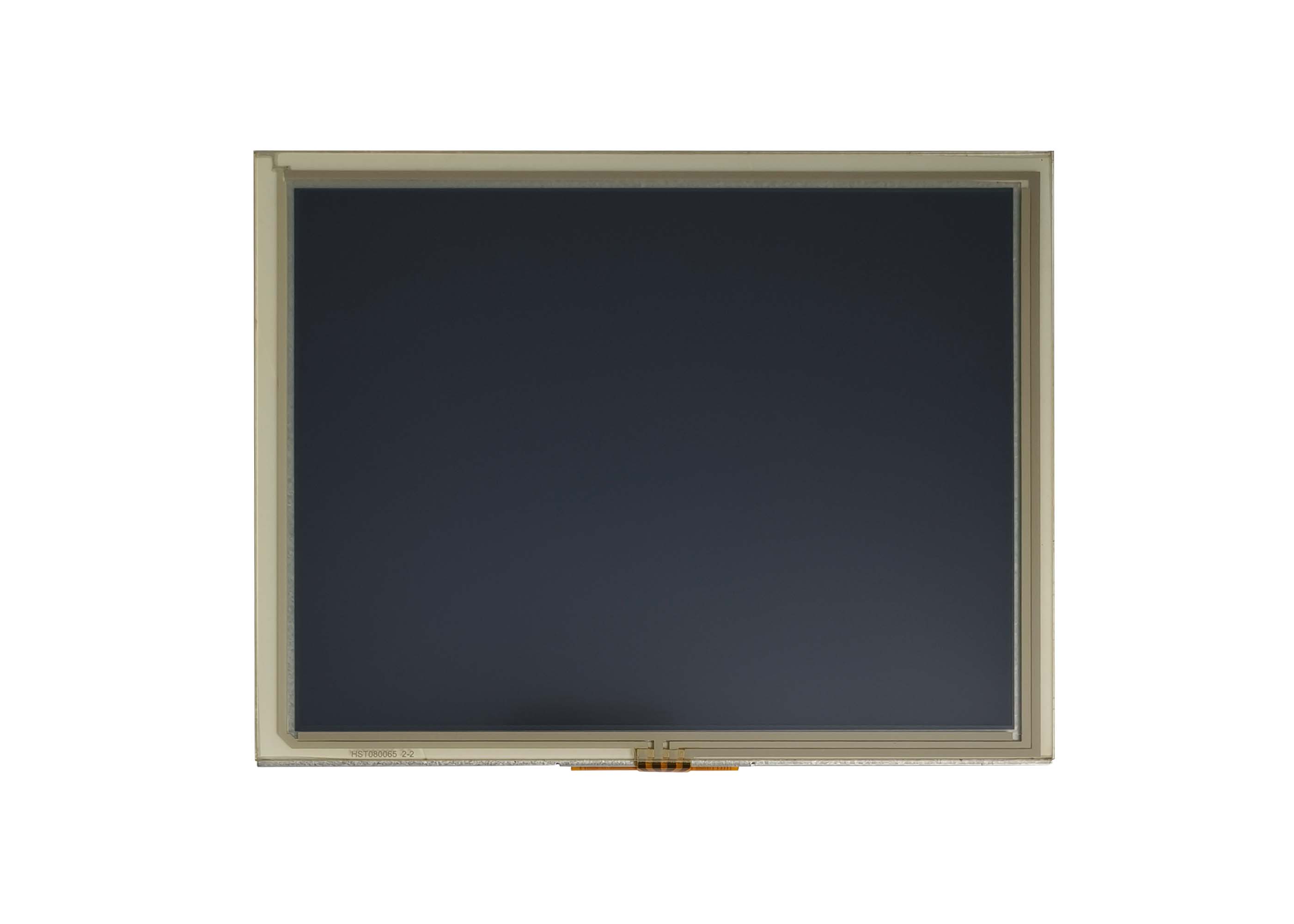
Which Logic Voltage, Common-Mode and Termination Requirements Apply?
Select LVDS electrical limits from the use case.
Define LVDS electrical limits in the project specification. Verify the released assembly under representative conditions with documented acceptance limits, traceable evidence, failure handling and change-control triggers.
Separate panel power, logic control levels, LVDS differential signaling and backlight power in the interface review. Check sequencing, tolerances, enable polarity and termination at the receiver. Never assume that a board labeled for LVDS automatically supplies the correct panel voltage or backlight current; those are independent requirements and a mismatch can damage the module before software diagnostics begin. Procurement should not convert an unverified capability into a commercial promise. Keep MOQ, lead time, price, lifetime and certification scope outside the technical conclusion until CDTech confirms them for the exact configuration. The RFQ can still request those items, but publication and sourcing decisions should label them as project-specific rather than typical values. The review should also cover foreseeable misuse and degraded states. Decide what the user sees after power interruption, communication loss, contamination or partial touch failure, and assign the response to the finished system. The component supplier can support testing without owning the complete safety decision.Which Pixel Clock, Blanking and Timing Range Does the Panel Require?
Select panel timing limits from the use case.
Define panel timing limits in the project specification. Verify the released assembly under representative conditions with documented acceptance limits, traceable evidence, failure handling and change-control triggers.
The controller must generate a timing set inside the panel's allowed operating window, including pixel clock, active resolution, sync polarity where relevant and horizontal and vertical blanking. Start from the panel's specified typical values and limits, not only the native resolution. Capture the actual signals during bring-up so intermittent artifacts are not misdiagnosed as cable or panel defects. For embedded display engineers, the practical deliverable is a line in the specification and an evidence item for LVDS LCD display. Record the owner on both sides, identify the sample or report revision, and state what triggers revalidation. If the supplier proposes a substitute material, panel revision, controller firmware or process change, the team can then assess impact before the approved baseline is altered. Close the review with an exceptions list. For each open LVDS LCD display item, record the assumption, risk, temporary control, responsible owner and date for closure. A sample should not silently become the production standard while unresolved deviations remain in email or meeting notes.How Should Connector, Cable, Shielding and Pin-One Control Be Verified?
Validate connector and cable on the released assembly.
Define connector and cable control in the project specification. Verify the released assembly under representative conditions with documented acceptance limits, traceable evidence, failure handling and change-control triggers.
Connector pin count does not define function. Two 30-pin or 40-pin interfaces can use different power rails, grounds, channel mappings, backlight connections, auxiliary signals and pin-one orientation. Create a point-to-point net list from controller to panel, verify mating parts and keying, inspect cable orientation, and perform continuity and short checks before the first powered test. Apply this point to the released assembly, not to an isolated demonstration. The LVDS LCD display review should use representative cables, enclosure geometry, software, optical stack and operating states. Keep raw results, photographs or plots, failures and corrective actions with the approval record. That evidence is more useful than a broad capability statement because it can be repeated after a design or supplier change. Use a golden sample only as a physical reference linked to controlled documents. It cannot replace numeric limits, configuration identity or a repeatable test. Store its revision, condition and approval record, and define when aging, damage or a design change makes the reference invalid.Safe bring-up sequence and diagnostic patterns
Medical display requirements start with the visual task and the consequence of a wrong or delayed interpretation. Diagnostic interpretation, clinical review, patient information and equipment control can demand different image-quality controls, calibration responsibilities and risk evidence. A bare LCD module is a component inside that system; it should not be described as a certified medical device or as satisfying finished-equipment obligations on its own. Write the acceptance method before requesting a sample. State setup, conditioning, observer or instrument position, operating mode, pass criteria and handling of borderline results. The same method should be usable at design validation, incoming inspection and change review. This prevents the OEM and supplier from approving different interpretations of the same LVDS LCD display requirement. Separate evidence needed for design selection from evidence needed for production release. Early engineering data may narrow options, while release evidence must represent the approved materials, tooling, process, firmware and assembly. This distinction keeps exploratory success from being overstated as production qualification.
Compatibility checklist before power-on
Electrical safety, EMC, isolation and power-quality responsibilities belong to the finished equipment architecture. The display supplier can provide component data, interface limits and test support, while the device manufacturer controls power supplies, grounding, cables, enclosure, protective measures and the final verification boundary. Record this division in the requirements matrix so a component report is not mistaken for system compliance. Procurement should not convert an unverified capability into a commercial promise. Keep MOQ, lead time, price, lifetime and certification scope outside the technical conclusion until CDTech confirms them for the exact configuration. The RFQ can still request those items, but publication and sourcing decisions should label them as project-specific rather than typical values. The review should also cover foreseeable misuse and degraded states. Decide what the user sees after power interruption, communication loss, contamination or partial touch failure, and assign the response to the finished system. The component supplier can support testing without owning the complete safety decision.| Panel | Mapping | Channels | Voltage | Timing | Connector |
|---|---|---|---|---|---|
| Exact panel, touch, cover, backlight and firmware baseline | Panel specification and controller configuration agree | Panel specification and controller configuration agree | Panel specification and controller configuration agree | Panel specification and controller configuration agree | Panel specification and controller configuration agree |
| Configuration installed in the representative system | Cable net list, sequencing and operating limits checked | Cable net list, sequencing and operating limits checked | Cable net list, sequencing and operating limits checked | Cable net list, sequencing and operating limits checked | Cable net list, sequencing and operating limits checked |
| Identified samples match the released documents | Current-limited bring-up with measured signals and patterns | Current-limited bring-up with measured signals and patterns | Current-limited bring-up with measured signals and patterns | Current-limited bring-up with measured signals and patterns | Current-limited bring-up with measured signals and patterns |
| New revision compared before production implementation | Interface review repeated after panel, board or cable revision | Interface review repeated after panel, board or cable revision | Interface review repeated after panel, board or cable revision | Interface review repeated after panel, board or cable revision | Interface review repeated after panel, board or cable revision |
FAQ / pre-publication query verification
What evidence should an OEM request for LVDS LCD display?
Request a revision-controlled drawing, interface and timing data, material and process scope, identified samples, validation reports, inspection criteria, traceability records and change-notification rules for the exact LVDS LCD display configuration. Certification scope, company data and project-specific commercial terms must be confirmed before publication or supplier approval.
Which requirement should be frozen before selecting LVDS LCD display?
Freeze intended use, system boundary, dimensions, interface, power, optical and touch stack, environment, operating states and acceptance methods before final LVDS LCD display selection. Early samples can explore risk, but production approval should refer to one released configuration and a documented disposition for every open deviation.
How should the released assembly be validated?
Validate the LVDS LCD display in the complete released assembly with representative cables, enclosure, grounding, software and environmental conditions. Record the setup, sample revision, raw results, failures, recovery and acceptance decision. Repeat affected tests after material, process, firmware or mechanical changes.
The useful outcome is not a broad claim about LVDS LCD display; it is a released requirement, a traceable configuration, a repeatable verification method and a controlled path for change. Keep component evidence inside the finished-equipment boundary, confirm current standards and certification scope, and treat commercial terms and lifetime data as project-specific until CDTech verifies them.